-
- Vacuum Seals
- Quartz Products
- Ceramics
- SiC Parts (CVD-SiC)
- Silicon Parts
- EB Components
- Vacuum Coating System
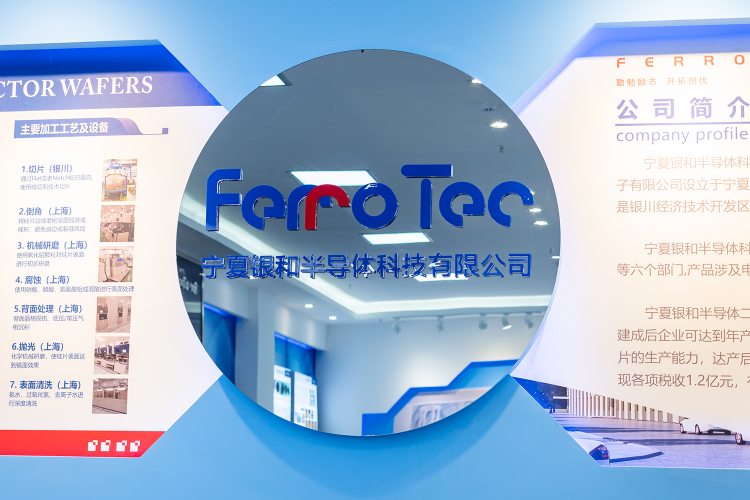
- Silicon Wafers
- Reclaim Wafer
- Process Tools Parts Cleaning
- Single Crystal Silicon Ingot Puller
- Quartz Crucibles
- Ferrofluid
- Thermo-electric Modules
- Chillers
- Thermistors
- Power Electronic Substrates
- Photovoltaic Silicon
- Saw Blades
- Industrial Knives and Cutters
- CMS
- Industrial Laundry Machine">
-
- Vacuum Seals
- Quartz Products
- Ceramics
- SiC Parts (CVD-SiC)
- Silicon Parts
- EB Components
- Vacuum Coating System
- Silicon Wafers
- Reclaim Wafer
- Process Tools Parts Cleaning
- Single Crystal Silicon Ingot Puller
- Quartz Crucibles
- Ferrofluid
- Thermo-electric Modules
- Chillers
- Thermistors
- Power Electronic Substrates
- Photovoltaic Silicon
- Saw Blades
- Industrial Knives and Cutters
- CMS
- Industrial Laundry Machine
- The Equipment Related Business
- Electronic Device Business
- Photovoltaic Related Products
- Other Related Business
The Equipment Related Business
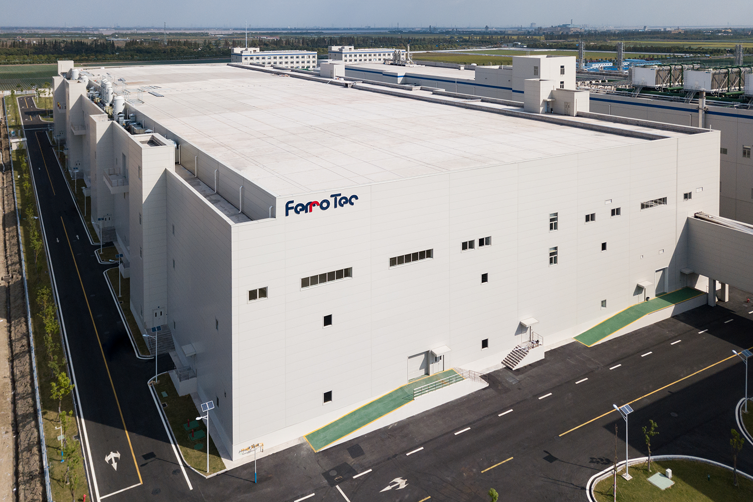
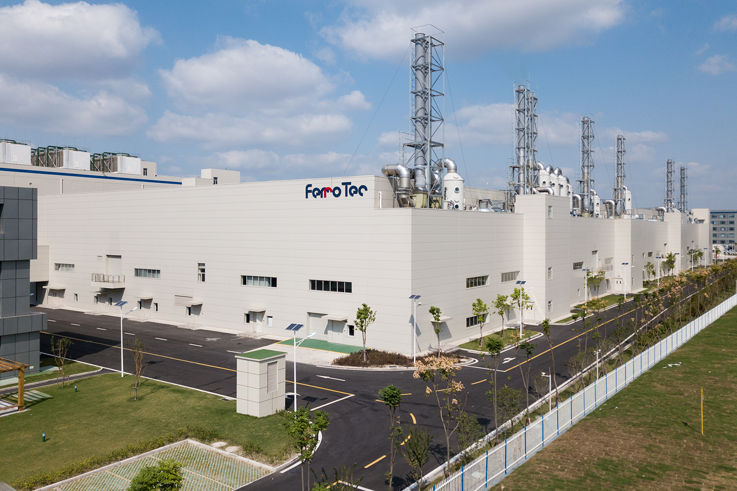
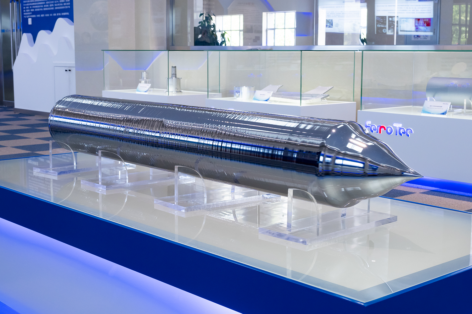
Silicon Wafers
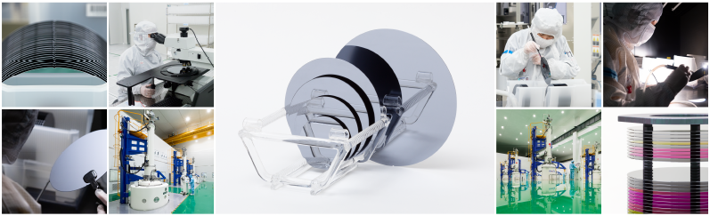
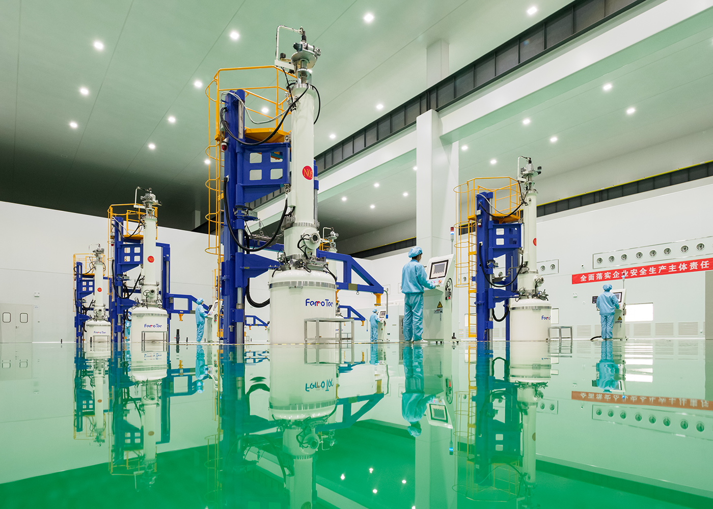
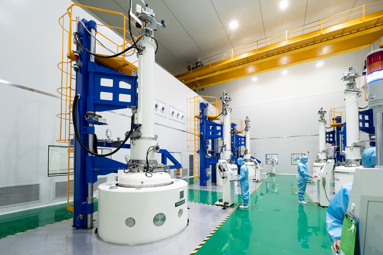
Integrated production from the singnle crystal ingots
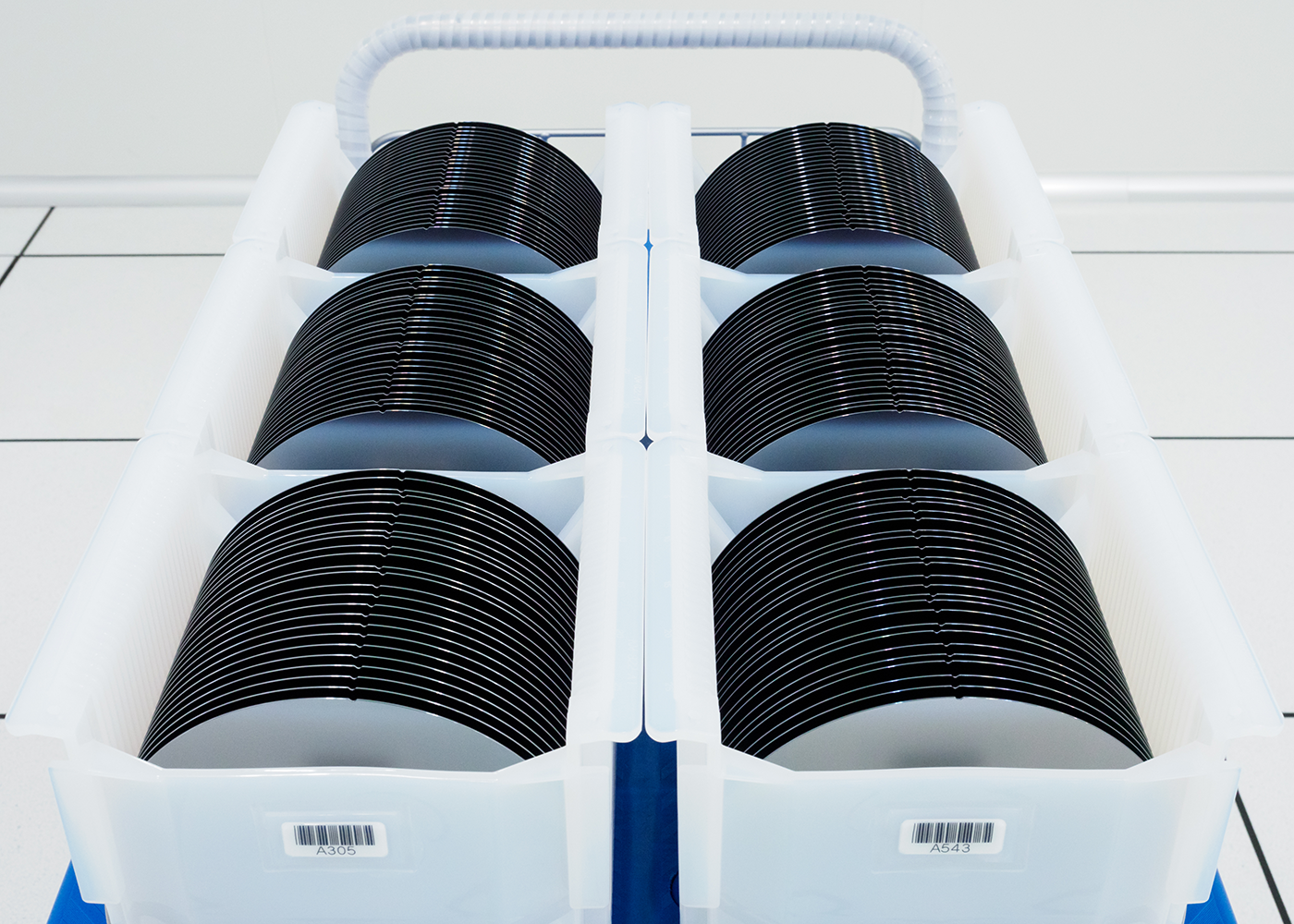
We produce small-diameter silicon wafers (12 inches or less) for semiconductors in an integrated manner ranging from single crystal ingots to wafer processing.We have established the global supply system mainly for the mass-produced wafers for bipolar integrated circuits, discrete circuits, and MEMS.
Map of the silicon wafer factories in China
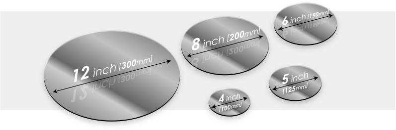
Silicon Wafer Sizes Offered
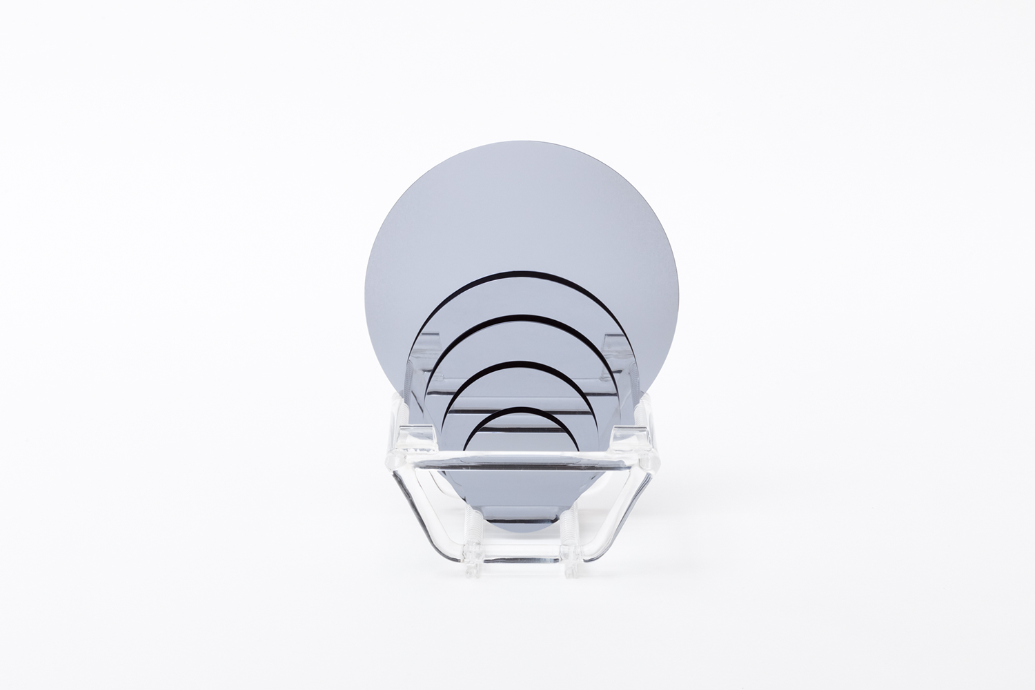
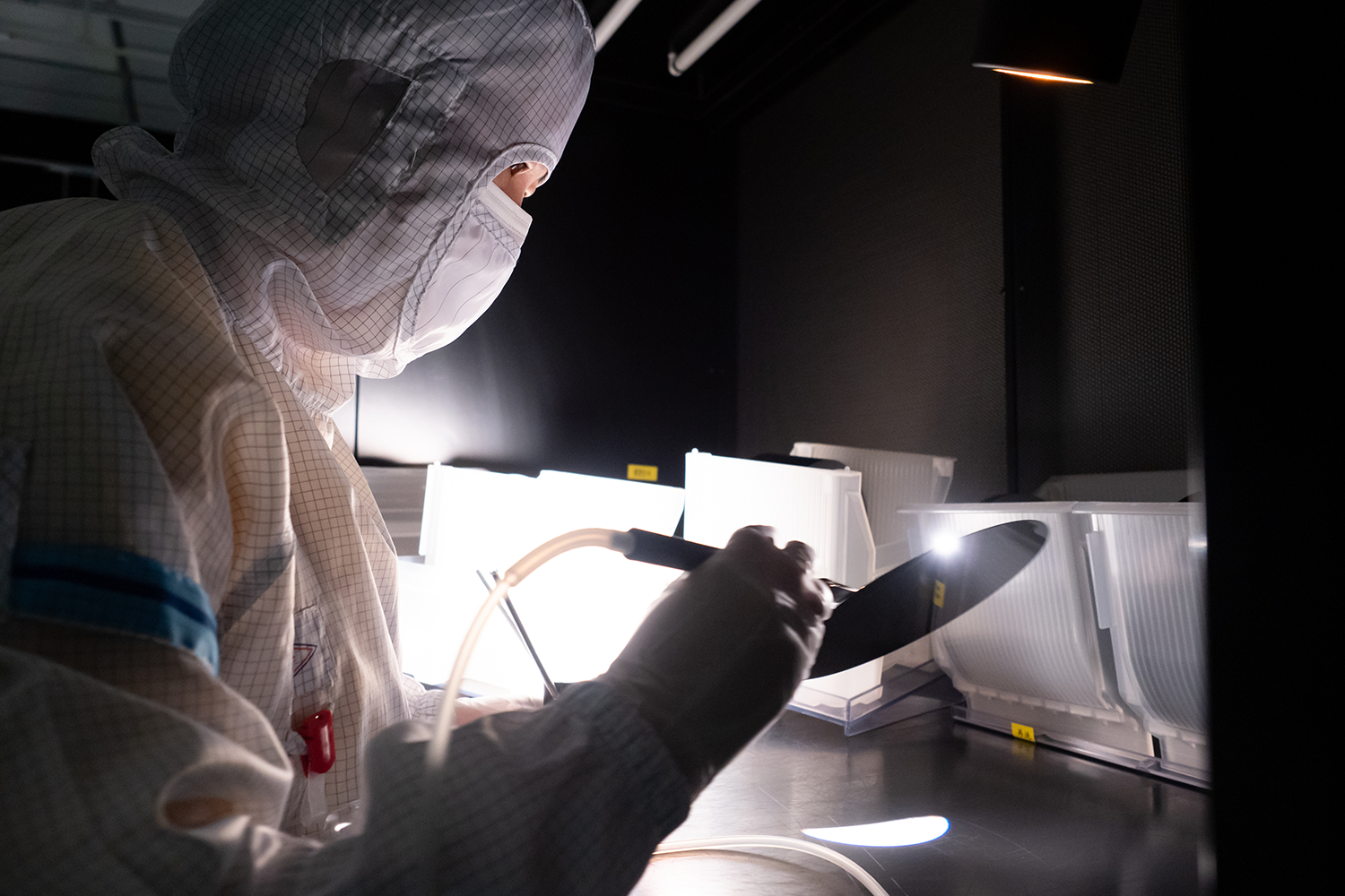
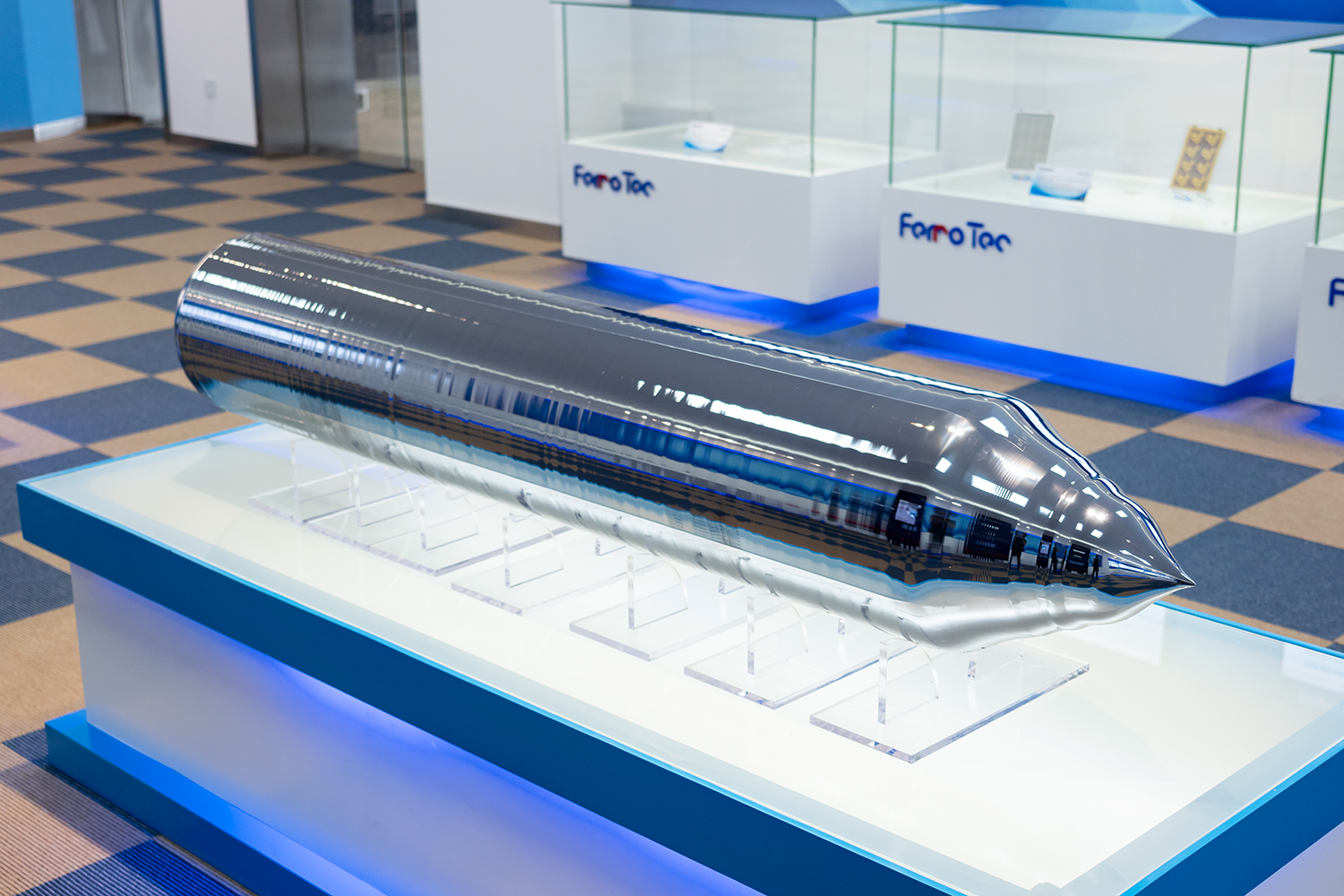
Polished Wafer
A Polished Wafer is made from a single-crystal silicon ingot which is thinly sliced and then mirror-finished on one side or both sides to produce high flatness and cleanability.Anneal Wafer
An Annealed Wafer is made by heating a Polished Wafer to a very high temperature in an argon atmosphere to provide an improved crystal integrity of the device formative layer and a gettering function for application to cutting-edge devices.COP Free Wafer
A COP Free Wafer can be used in advanced devices in which oxygen precipitates and a collection of pores or COPs (Crystal Originated Particles), which degrade the breakdown voltage of a gate oxide film and increase junction leakage currents, are removed by controlling crystal growth.Substrate for Epi Wafer
As a substrate for Epi Wafers, this wafer accommodates various types of dopants (boron, phosphorus, arsenic, and antimony) that control the characteristics of the device.Epi Wafer
An Epi Wafer is made from a single crystal silicon that grows on the surface of a Polished Wafer by a vapor phase epitaxy method, featuring a superior quality as a substrate for discrete semiconductors and MOS-ICs.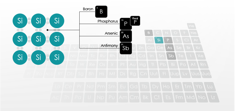
End products
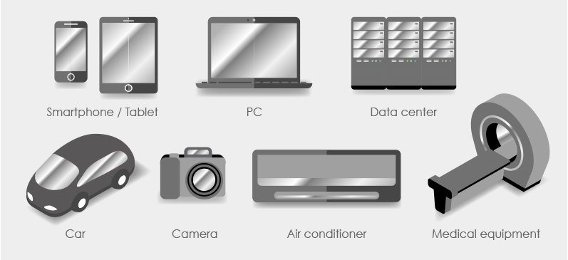
These wafers are used in products such as cars, smartphones, PCs, industrial equipment, server/cloud centers, home appliances (air conditioners, wearable terminals), and medical equipment.

Silicon Wafer Business Group
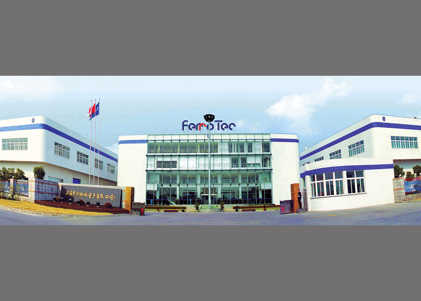
FerroTec Shanghai
Shanghai Ferrotec Shanghai Semiconductor Wafer Co., Ltd.

- Type
- Small diameter
- Medium diameter
- Wafer size
- 4, 5, and 6 inches
- 8 inches
- Monthly production amount
- 400 K / Month
- 100 K / Month
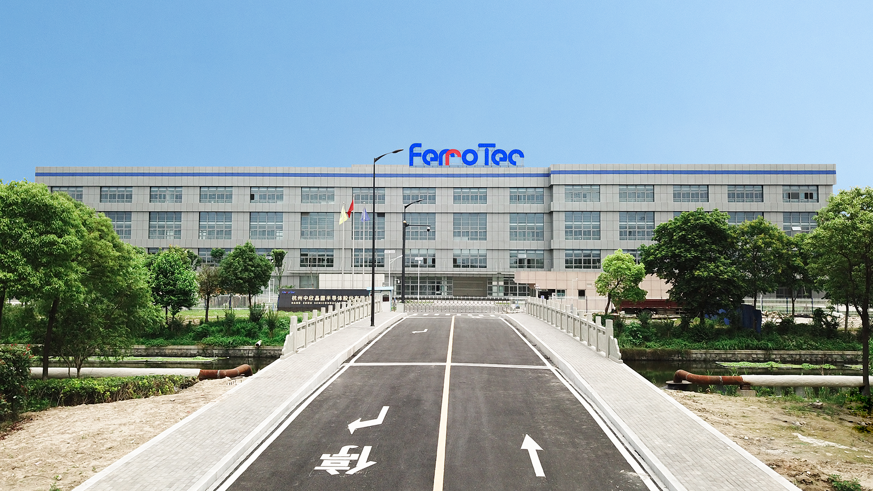
FerroTec Hangzhou
Hangzhou Hangzhou Semiconductor Wafer Co., Ltd.
- Type
- Medium diameter
- Large diameter
- Wafer size
- 8 inches
- 12 inches
- Monthly production amount
- 350 K / Month
- 30 K / Month
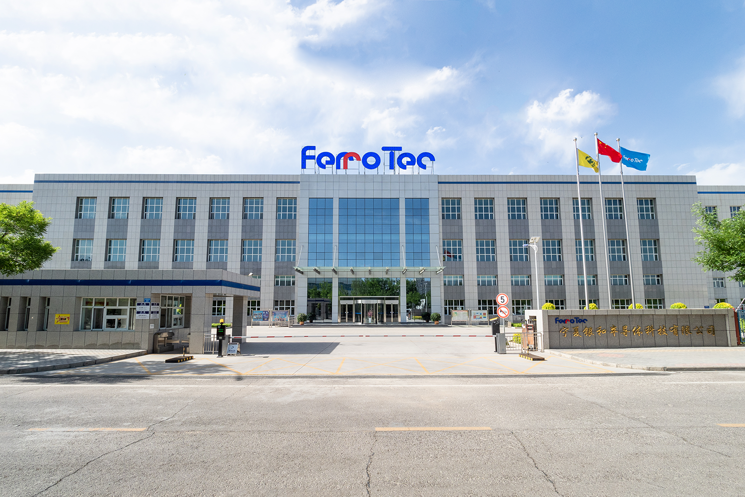
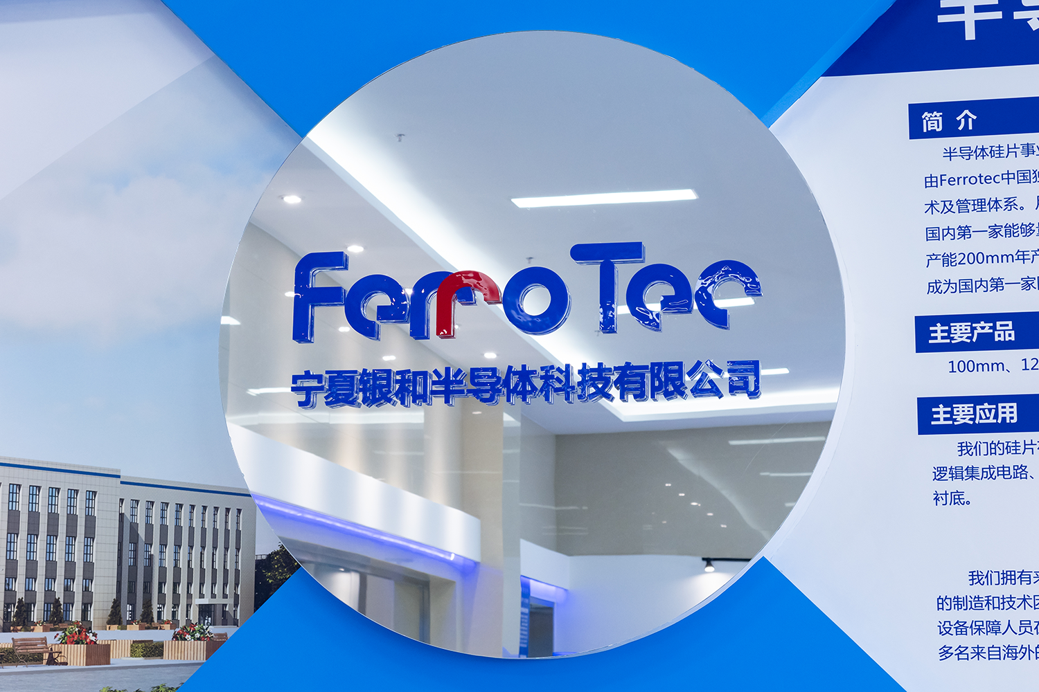
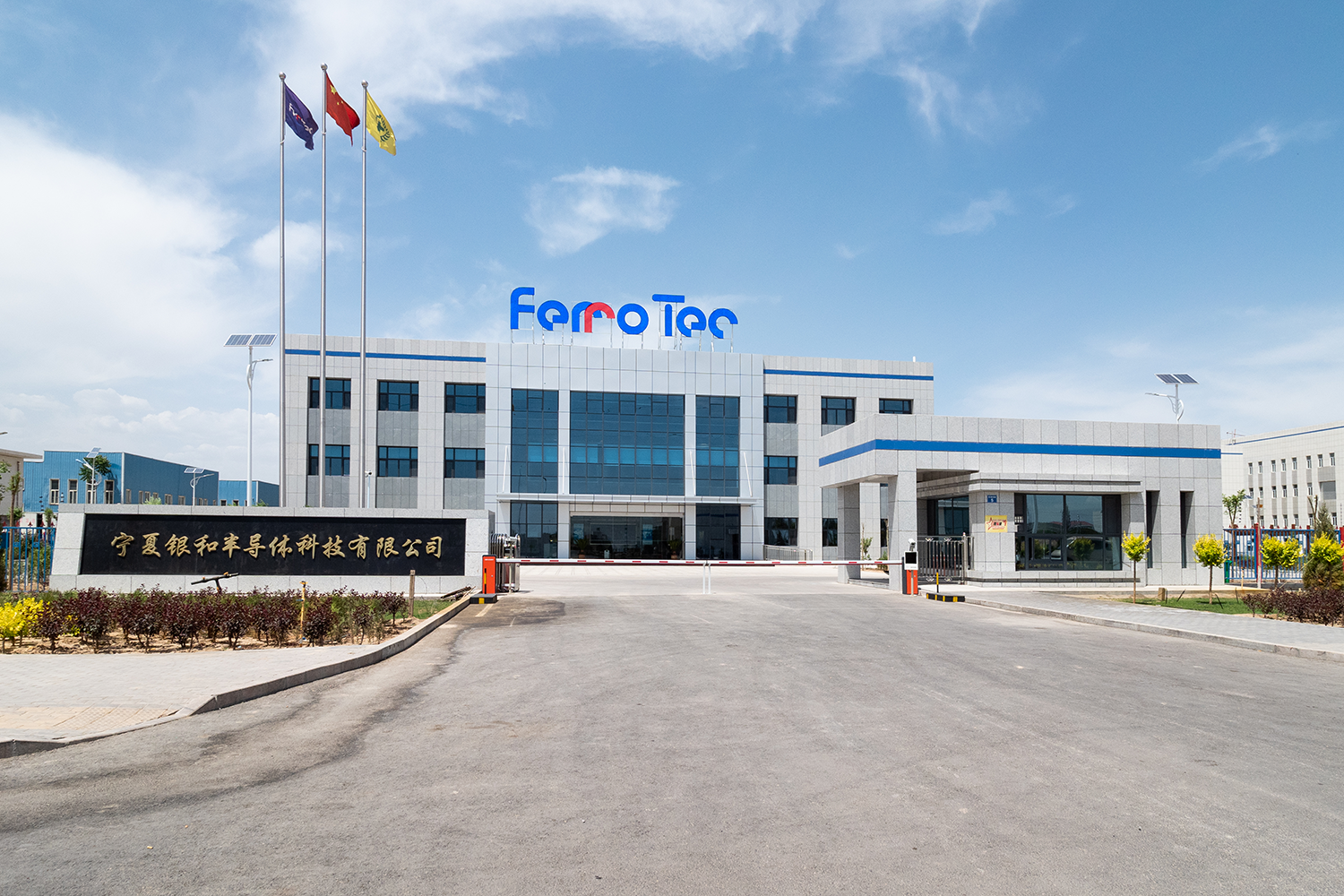
FerroTec Ningxia
Yinchuan Ferrotec (Ningxia) Semiconductor Technology Co., Ltd.
1st Factories
2nd Factories
- Ingot
- 4, 5, 6, 8, 12 inches
- Adress
- 1st Factories
- No.28 West Guangming Road, Yinchuan Economic and Technological Development Zone, Ningxia, 750021, P.R. China
-
Map
- 2nd Factories
- No.5 West Baohu Road, Yinchuan Economic and Technological Development Zone, Ningxia, 750021, P.R. China
-
Map
Industries that use these technologies
| Audio | Automotive | Electronics | Medical Equipment | Home Appliance | Other Industries | |
|---|---|---|---|---|---|---|
| The Equipment Related Business | ||||||
| Vacuum Seals |
|
|
|
|||
| Quartz Products |
|
|
|
|||
| Ceramics |
|
|
|
|||
| SiC Parts (CVD-SiC) |
|
|
|
|
||
| Silicon Parts |
|
|
|
|||
| EB Components |
|
|
||||
| Vacuum Coating System |
|
|
||||
| Silicon Wafers |
|
|||||
| Process Tools Parts Cleaning | ||||||
| Electronic Device Business | ||||||
| Ferrofluid |
|
|
|
|
|
|
| Thermo-electric Modules |
|
|
|
|
||
| Power Electronic Substrates |
|
|
|
|
||